Excimer Laser Annealing System

Excimer Laser Annealing Systemfor High-resolution Panels
YIELDSCAN ELA
Excimer Laser Annealing System YIELDSCAN ELA

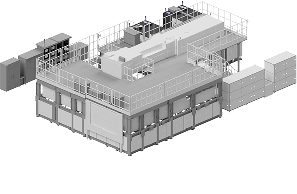
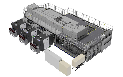
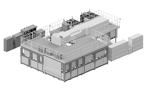
The Excimer Laser Annealing (ELA) system converts amorphous silicon film on a glass substrate into a polycrystalline silicon one. The low-temperature polycrystalline silicon is generally used in the TFT (Thin Flat Transistor) of the high-resolution panels. ELA System is essential for the production of high-resolution panels, such as smartphones, automobile monitor and portable gaming devices.

Features

Applicable Fields and Uses

Application: Si Crystallization
Industry: FPD (Smartphone, In-vehicle, VR, tablet, laptop, medical, etc.)

Sales Records

Since 1995, we have installed over 240 systems to display companies in China, Japan, South Korea, Taiwan and Singapore, as one of the top manufacturers of the ELA system.


Excimer Laser Annealing System
(Gen 4)

Excimer Laser Annealing System

Excimer Laser Annealing System
(Gen 6)

Excimer Laser Annealing System
The world's First

Large-Scale
Excimer Laser Annealing System
(supporting 8th-Generation Substrates)

Large-Scale excimer laser annealing system

Specification

G4.5 G6 G8.6 G10.5
Applications Mobile, VR
Automotive or
In-Vehicle
Mobile, VR,
Foldable
Automotive or
In-Vehicle
OLED Tablet & Foldable
TV & Monitor
OLED Tablet & Foldable
TV & Monitor
Substrate size [mm] 730 × 920 1,500 × 1,850 2,290 × 2,620 2,940 × 3,370
TFT LTPS LTPS LTPS BG-LTPS
Laser Vyper Vyper,
Twin-Vyper
Twin-Vyper Tri-Vyper
Optical system LB750.2 LB750.2,
LB1000
LB1300-G8 LB1500XL
Stage StiFloat
or
Air bearing stage
StiFloat
or
Air bearing stage
StiFloat StiFloat

Process Examples

Full scanning of amorphous substrate to LTPS

Full scanning of amorphous substrate to LTPS

StiFloat

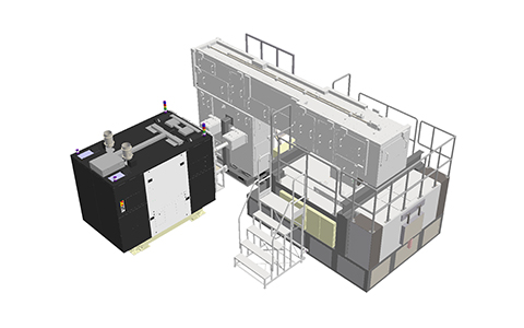
Features of the JSW-FELA*1 system with a float-type stage
The glass substrate (substrate) is transported with almost no contact, since the contact on the back of the substrate is limited to the minimum by floating the substrate with airflow.

  1. Capable of handling large substrates (up to G10.5), achieving a high-performance, stable ELA process
    Our original substrate-transfer technology provides the most optimal ELA process.
  2. Stable laser irradiation process by improving velocity stability during substrate transport
    Non-contact frictionless transport provides speed stability for the stage, reducing uneven irradiation.
  3. Expanding process margin by increasing flatness of substrates in irradiation area
    The JSW-FLEA system structurally transports only a substrate and increases the flatness of substrates in irradiation area compared with the VC*2 method since only a limited irradiation area needs to be planarized. Therefore, during laser irradiation, the substrates are processed at a constant height within the focal range of the laser beam.
  4. Reduction of irradiation Mura
    N2 flow Mura and Mura caused by VCs, which have been issues with conventional ELA systems, are reduced.
    · Airflow Mura
    The N2 airflow in the laser irradiation area is optimally designed using airflow control technology, taking advantage of the float-type structure.
    · Mura caused by VCs
    Due to the lack of contact with VCs, the backside of the substrate is not affected by VC grooves, etc., and irradiation Mura caused by VCs does not occur.
  5. Reduction of ESD*3
    Since the substrate is transported in an almost non-contact state in the JSW-FELA system, static electricity caused by contact is not generated.
    In addition, components in contact with substrates such as substrate-gripping parts are made of materials that prevent ESD generation.
  6. Reduction of particle
    In the JSW-FELA system, only substrates are transported in a state of non-contact, so particles spread and adhered to the substrate are extremely small compared to conventional systems.

*1 FELA: Float-type ELA system
*2 VC: Substrate holding stage of vacuum-suction type
*3 ESD: Electro-Static Discharge


*YIELDSCAN: Japanese Registered Trademark (Number 6553271), StiFloat: Japanese Registered Trademark (Number 6576709)

Page top