As flat-panel displays become more high-definition and semiconductor circuits more highly integrated, mass production systems are increasingly required to provide a sophisticated performance.
We are constantly striving to improve our technological expertise by developing optical designs optimized for the systems that customers need, and by creating various fine-tuned control technologies.
We are able to make suggestions for suitable optical systems for various laser processes.
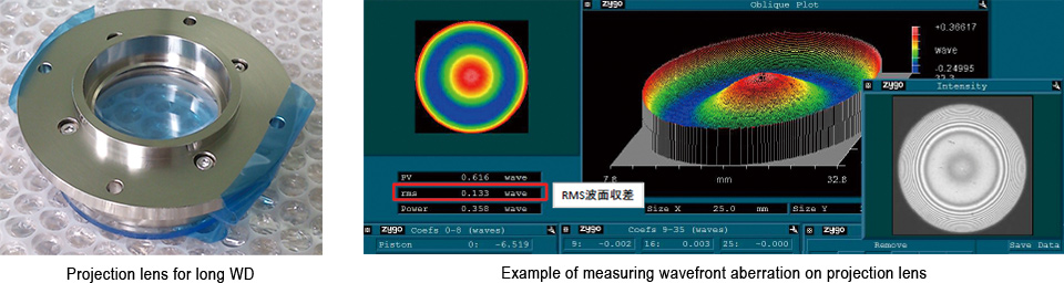
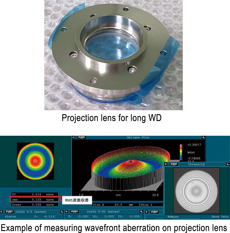
Projection lens for reduced-size projection system with long working distance (WD)
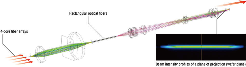
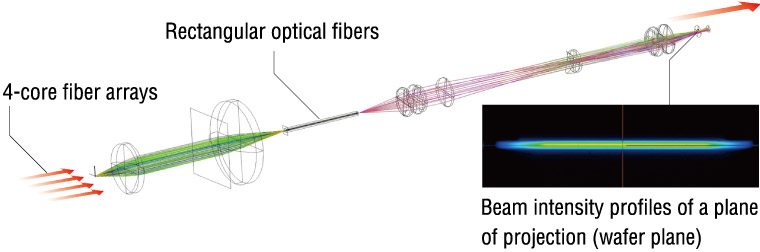
Optical system that changes shape from several infrared laser diodes to line beam combining laser outputs
The high-precision transport technology is necessary for workpieces of glass substrates or semiconductor wafers with cutting-edge laser processing.
We build an optimal stage transport system considered characteristics for various laser processes and optical systems, and then set and launch our products at customers' manufacturing plants.
We have laser inter ferometers, auto-collimators and levelers to guarantee the accuracy of high-precision stages, and manage them for stable operation of our products. Also, a control program is essential to take advantage of the performance of high-precision stages. We provide stage transport systems with stable operation, using total control technology combined with motion controllers, alignment optical systems, and displacement sensors.
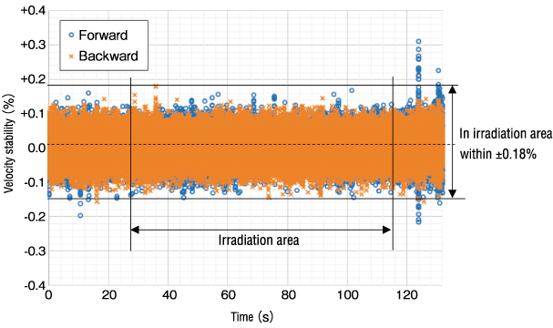
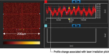
It is indispensable that the workpiece transport velocity remains stable in the laser annealing process.
Measurement result example of velocity stability is shown.
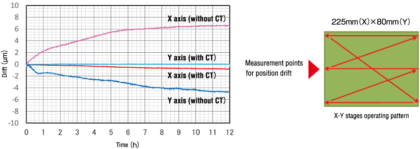
Even in a long-process time case, apply countermeasure technology to maintain high absolute positioning accuracy.
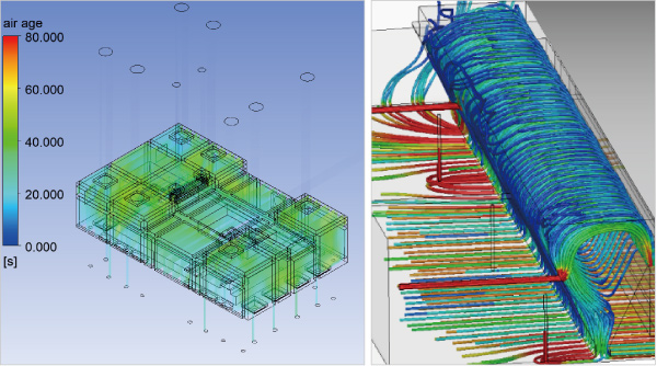
With the needs of high-resolution flat-display panels, stricter process management is important. Our accumulated technology over analysis of irradiation atmosphere and air flow in chamber assuredly improves customer's production yield.
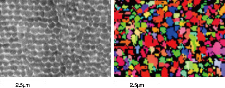
We have been developing a process for laser cr ystallization of amorphous silicon and engaged in R&D activities of analysis technique. Our various analysis technique will provide customers with solutions.
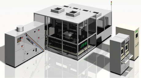
JSW Aktina Syetem has developed not only the ELA system but also various t ypes of laser annealing systems used by end users.
JSW Aktina Syetem proposes annealing processes and system suitable for the process.
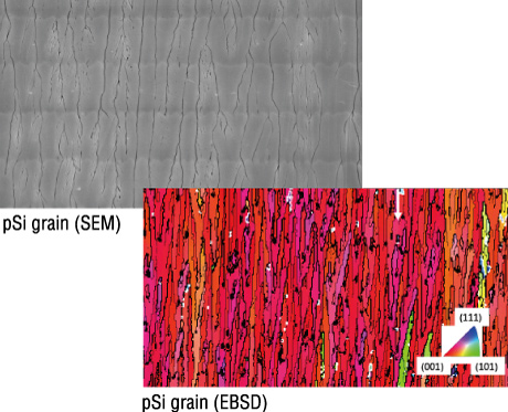
When the aSi film is melted and solidified by irradiating it with a laser, the Si film grows laterally along the in-plane (Lateral solidification). SLS is a method of controlling the starting point of crystal growth by irradiating a mask pattern with a laser to form a pSi film with a uniform grain size on the whole surface of the substrate.
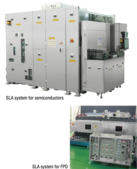
JSW Aktina System has developed a system for the SLS method and delivered it to display manufactures in 2004. The SLS device irradiates the aSi film on the glass substrate with a 300-W excimer laser using a projection lens. It is equipped with various functions and know-how for stabilizing the optical system and controlling the stage position in high-power lasers.
The SLA system was developed to continuously crystallize the aSi film in one direction and was delivered to display manufacturers in 2007.
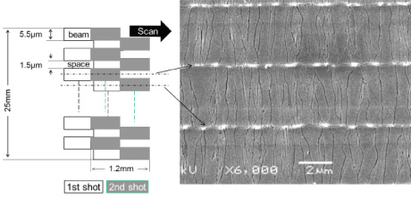
The SLA system is equipped with a solid-state green laser with variable pulse width (300 to 1200 ns), and by scanning and annealing a line beam with a beam width of 8 µm in one direction, a large particle size pSi with uniform surface orientation is formed. SLA systems has also been expanded to semiconductor applications and is still used in the manufacture of CMOS image sensors.
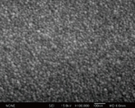
The R-SPC system is used for crystallizing aSi film by solid phase growth, and was delivered to display manufacturers in 2010. The R-SPC system scans a continuous wave (CW) laser beam onto the aSi film at high speed. Therefore, the heating time can be controlled in the microseconds order, and a high-quality fine pSi film (grain size: 10 to 20 nm, mobility: 2 to 5 cm2 / V・s) can be applied to the whole surface of the G2 substrate at the optimum heating time.