 MLA
MLA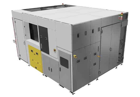
The Micro Laser Annealing (MLA) system irradiates a microbeam controlled area by a mask pattern to a specific position on the substrate. With the MLA system, thin films of minute area in the micro-meter order can be crystallized, activated, made highly dielectric, etc. without affecting the base substrate with heat.
Application: Crystallization/Activation/High dielectricization
Industry: LCD, Semiconductor, Other Industrial Devices
It is used in semiconductor mass-production factories.
| Workpiece size | 6 inch, 8 inch | |
|---|---|---|
| Irradiation positioning accuracy | ±1 µm | |
| Laser | Wavelength | 248 nm |
| Pulse width | 20 ns | |
| Power | 30 W | |
| Process throughput | 3 min/wafer (6 inch) | |
| Irradiation | Mask Projection, Top flat beam Min Sq 10 µm/Max Sq 2.4 mm Several pattern on 9 inch Mask |
|
| System dimensions [mm] | W 3,200 x D 4,000 x H 2,500 (With automatic wafer handling) |
|
*YIELDSCAN: Japanese Registered Trademark (Number 6553271)
