 SLA
SLA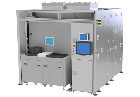
Due to the increasing complexity of semiconductor device structures, there is a growing demand for heat-treatment processes that target the local surface layer of the device. Our Laser Annealing system meets such demands, which are now mainly used for the mass production of high-performance image sensors. We are also engaging in R&D activities in order to expand the application of our system.
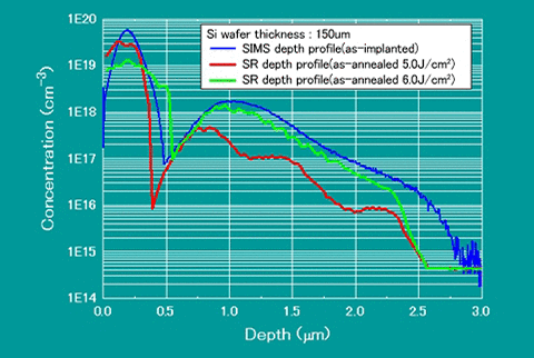
Simultaneous shallow and deep areas activation
(Ion implantation condition: P/750 keV, B/40 keV)
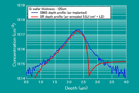
Only deep-area activation
(Ion implantation condition: P/3 MeV)
Application: Activation
Industry: Semiconductor (image sensor, etc.)
We have sold the system used for an activation process to a semiconductor manufacturing company.
*YIELDSCAN: Japanese Registered Trademark (Number 6553271)
