WHAT'S
JSW AKTINA?
What does JSW AKTINA do?
What is a Laser Annealing System?
What is a Laser Annealing System?
WHAT IS AKTINA?
What does
JSW AKTINA do?
JSW AKTINA do?
JSW Aktina is a prominent laser systems manufacturer representing Japan.
As a pioneer in excimer laser annealing systems, JSW Aktina has been at the forefront of the FPD and semiconductor industries for many years. Through our commitment to innovative technology development, we contribute to the manufacturing of a wide range of products that play an essential role in everyday life.
in Numbers
For nearly 30 years since the launch of our first laser annealing system, JSW Aktina has been delivering cutting-edge solutions to customers worldwide. The technological innovations driven by JSW Aktina will continue to evolve, contributing to the growth of industries worldwide.
AKTINA's advantage
- Contributing to global industrial development -
-
We manufactured the globally first-ever mass-production ELA system
(first generation model)0*Generation 1 substrate size: 300 mm×400 mm -
We manufactured the globally first-ever Generation 8.6 mass-production ELA system0*Generation 8.6 substrate size: 2,290 mm×2,620 mm
-
Remarkable achievement:
Excimer Laser
Annealing Systems
Delivered0+*As of 2024
Work Life Balance
- A comfortable workplace -
-
Number of paid days off
Number of days granted:0 days*Granted 11 days in the first year of employment
Granted 22 days from the second year onwards -
Average years
of service0 years*End of March 2025 -
New employee
retention rate (3 years)0%*End of March 2025
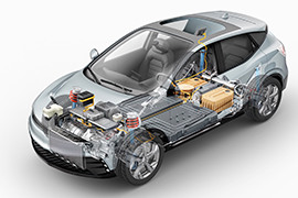
Contributing to industries across diverse fields worldwide.


- Communications
and AI - Power
Semiconductors - LCD/OLED
- Sensor
- Process
Machinery - Medical Care
WHAT IS LASER ANNEALING?
WHAT IS LASER ANNEALING?
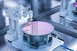
Laser annealing enables precise heat treatment exclusively on the surface of wafers or glass substrates, allowing for selective surface modification processes such as crystallization, alloying, and activation.
Among various technologies, the line-beam excimer laser annealing system developed by JSW Aktina stands out for its ability to perform uniform annealing over a wide area. This system has also been widely adopted in the mass production of semiconductor and FPD devices.
- Crystallization process
-
-
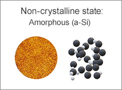
The dark gray spheres indicate silicon atoms, while the white spheres represent hydrogen. In the initial amorphous state, atoms are arranged in a random, disordered structure.
-

-
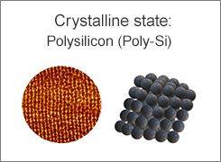
Through the laser annealing process, the atoms align themselves regularly and transform into a crystalline state.
-
- Si/SiC Alloying process