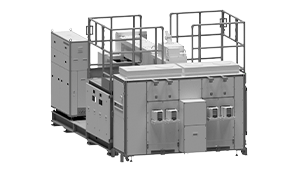
This system is designed for silicidation by processing metal films deposited on SiC wafers.
Leveraging world-class high-power gas laser control technology, it achieves industry-leading uniformity combined with ultra-high-speed scanning.
It has become an essential solution for advancing the energy efficiency and miniaturization of next-generation power semiconductors.
Laser Annealing System for ActivationYIELDSCAN SLA
Laser Annealing
Image Sensor
Thermal Process
Pulse Control
Activation
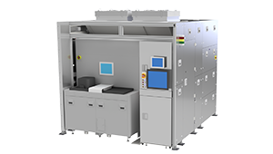
This system is used in semiconductor device manufacturing for localized thermal processing, where only specific surface areas are selectively heated. It is utilized for activation in targeted areas and has been widely adopted in the mass production of advanced image sensors.
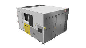
This system irradiates the substrate with finely controlled micro-beams using a mask pattern, enabling localized processing of thin films at the micrometer scale, such as crystallization, activation, and high dielectricization without raising the temperature of the base substrate.
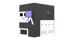
Various semiconductor processes for Si/SiC wafers (crystallization, activation, alloying, LLO, etc.) play an important role in each manufacturing process of semiconductor devices.
The compact, space-saving processing system is used for a wide range of applications such as sample verification and small-lot production.
This system is used to convert amorphous silicon films deposited on glass substrates into polycrystalline silicon.
With its unique technology recognized globally, it plays a crucial role in the production of high-definition panels used in smartphones, PCs, and other advanced electronic devices worldwide.
This system is designed to detach flexible displays from carrier glass using laser irradiation.
By utilizing a short-wavelength UV laser, it effectively prevents damage to the device during the detachment process.
This system is capable of performing multiple processing steps such as cutting, detaching, and cleaning of films and sheets.
It is primarily used in the manufacturing process of flexible displays.
This system performs high-precision laser heat treatment on a variety of materials, including resins and glass.
It enables localized thermal processing and is widely adopted in the manufacturing of electronics devices as well as across various industrial applications.